- 您现在的位置:买卖IC网 > Sheet目录3891 > PIC18C801T-I/L (Microchip Technology)IC MCU ROMLESS A/D PWM 84PLCC
2007 Microchip Technology Inc.
Preliminary
DS39625C-page 143
PIC18F2585/2680/4585/4680
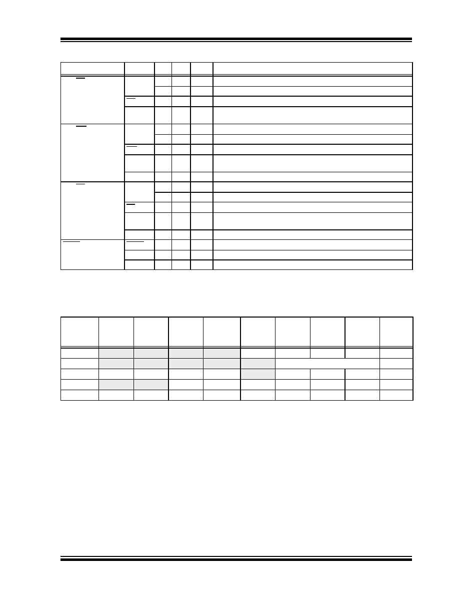
TABLE 10-9:
PORTE I/O SUMMARY
TABLE 10-10: SUMMARY OF REGISTERS ASSOCIATED WITH PORTE
Pin Name
Function
I/O
TRIS Buffer
Description
RE0/RD/AN5
RE0
OUT
0
DIG
LATE<0> data output.
IN
1
ST
PORTE<0> data input.
RD
IN
1
TTL
PSP read enable input.
AN5
IN
1
ANA
A/D input channel 5. Enabled on POR, this analog input overrides the
digital input (read as clear – low level).
RE1/WR/AN6/C1OUT RE1
OUT
0
DIG
LATE<1> data output.
IN
1
ST
PORTE<1> data input.
WR
IN
1
TTL
PSP write enable input.
AN6
IN
1
ANA
A/D input channel 6. Enabled on POR, this analog input overrides the
digital input (read as clear – low level).
C1OUT
OUT
0
DIG
Comparator 1 output.
RE2/CS/AN7/C2OUT
RE2
OUT
0
DIG
LATE<2> data output.
IN
1
ST
PORTE<2> data input.
CS
IN
1
TTL
PSP chip select input.
AN7
IN
1
ANA
A/D input channel 7. Enabled on POR, this analog input overrides the
digital input (read as clear – low level).
C2OUT
OUT
0
DIG
Comparator 2 output.
MCLR/VPP/RE3
MCLR
IN
x
ST
External Reset input. Disabled when MCLRE Configuration bit is ‘1’.
VPP
IN
x
ANA
High-voltage detection; used by ICSP operation.
RE3
IN
1
ST
PORTE<3> data input. Disabled when MCLRE Configuration bit is ‘0’.
Legend:
PWR = Power Supply; OUT = Output; IN = Input; ANA = Analog Signal; DIG = Digital Output; ST = Schmitt Buffer Input;
TTL = TTL Buffer Input
Name
Bit 7
Bit 6
Bit 5
Bit 4
Bit 3
Bit 2
Bit 1
Bit 0
Reset
Values
on page
PORTE(3)
—
—RE3(1,2)
RE2
RE1
RE0
LATE(2)
—
LATE Data Output Register
TRISE(3)
IBF
OBF
IBOV
PSPMODE
—
TRISE2
TRISE1
TRISE0
ADCON1
—
VCFG1
VCFG0
PCFG3
PCFG2
PCFG1
PCFG0
CMCON(3)
C2OUT
C1OUT
C2INV
C1INV
CIS
CM2
CM1
CM0
Legend: — = unimplemented, read as ‘0’. Shaded cells are not used by PORTE.
Note 1:
Implemented only when Master Clear functionality is disabled (MCLRE Configuration bit = 0).
2:
RE3 is the only PORTE bit implemented on both PIC18F2X8X and PIC18F4X8X devices. All other bits are
implemented only when PORTE is implemented (i.e., PIC18F4X8X devices).
3:
These registers are unimplemented on PIC18F2X8X devices.
发布紧急采购,3分钟左右您将得到回复。
相关PDF资料
PIC18C658T-I/L
IC MCU OTP 16KX16 CAN 68PLCC
PIC18C658T-E/L
IC MCU OTP 16KX16 CAN 68PLCC
PIC16C925T-I/L
IC MCU OTP 4KX14 LCD DVR 68PLCC
PIC12F675-E/P
IC MCU CMOS 1K FLASH W/AD 8-DIP
PIC18C858T-E/L
IC MCU OTP 16KX16 CAN 84PLCC
PIC16F636-I/SL
IC PIC MCU FLASH 2KX14 14-SOIC
PIC18LC658T-I/L
IC MCU OTP 16KX16 CAN 68PLCC
PIC18LC801T-I/L
IC MCU ROMLESS A/D PWM 84PLCC
相关代理商/技术参数
PIC18C801T-I/PT
功能描述:8位微控制器 -MCU 2MB 1536 RAM 37I/O RoHS:否 制造商:Silicon Labs 核心:8051 处理器系列:C8051F39x 数据总线宽度:8 bit 最大时钟频率:50 MHz 程序存储器大小:16 KB 数据 RAM 大小:1 KB 片上 ADC:Yes 工作电源电压:1.8 V to 3.6 V 工作温度范围:- 40 C to + 105 C 封装 / 箱体:QFN-20 安装风格:SMD/SMT
PIC18C858-E/L
功能描述:8位微控制器 -MCU 32KB 1536 RAM 68I/O RoHS:否 制造商:Silicon Labs 核心:8051 处理器系列:C8051F39x 数据总线宽度:8 bit 最大时钟频率:50 MHz 程序存储器大小:16 KB 数据 RAM 大小:1 KB 片上 ADC:Yes 工作电源电压:1.8 V to 3.6 V 工作温度范围:- 40 C to + 105 C 封装 / 箱体:QFN-20 安装风格:SMD/SMT
PIC18C858-E/PT
功能描述:8位微控制器 -MCU 32KB 1536 RAM 68I/O RoHS:否 制造商:Silicon Labs 核心:8051 处理器系列:C8051F39x 数据总线宽度:8 bit 最大时钟频率:50 MHz 程序存储器大小:16 KB 数据 RAM 大小:1 KB 片上 ADC:Yes 工作电源电压:1.8 V to 3.6 V 工作温度范围:- 40 C to + 105 C 封装 / 箱体:QFN-20 安装风格:SMD/SMT
PIC18C858EPT
制造商:MICRO CHIP 功能描述:New
PIC18C858-I/L
功能描述:8位微控制器 -MCU 32KB 1536 RAM 68I/O RoHS:否 制造商:Silicon Labs 核心:8051 处理器系列:C8051F39x 数据总线宽度:8 bit 最大时钟频率:50 MHz 程序存储器大小:16 KB 数据 RAM 大小:1 KB 片上 ADC:Yes 工作电源电压:1.8 V to 3.6 V 工作温度范围:- 40 C to + 105 C 封装 / 箱体:QFN-20 安装风格:SMD/SMT
PIC18C858-I/PT
功能描述:8位微控制器 -MCU 32KB 1536 RAM 68I/O RoHS:否 制造商:Silicon Labs 核心:8051 处理器系列:C8051F39x 数据总线宽度:8 bit 最大时钟频率:50 MHz 程序存储器大小:16 KB 数据 RAM 大小:1 KB 片上 ADC:Yes 工作电源电压:1.8 V to 3.6 V 工作温度范围:- 40 C to + 105 C 封装 / 箱体:QFN-20 安装风格:SMD/SMT
PIC18C858T-E/L
功能描述:8位微控制器 -MCU 40MHz 16K OTP RoHS:否 制造商:Silicon Labs 核心:8051 处理器系列:C8051F39x 数据总线宽度:8 bit 最大时钟频率:50 MHz 程序存储器大小:16 KB 数据 RAM 大小:1 KB 片上 ADC:Yes 工作电源电压:1.8 V to 3.6 V 工作温度范围:- 40 C to + 105 C 封装 / 箱体:QFN-20 安装风格:SMD/SMT
PIC18C858T-E/PT
功能描述:8位微控制器 -MCU 32KB 1536 RAM 68I/O RoHS:否 制造商:Silicon Labs 核心:8051 处理器系列:C8051F39x 数据总线宽度:8 bit 最大时钟频率:50 MHz 程序存储器大小:16 KB 数据 RAM 大小:1 KB 片上 ADC:Yes 工作电源电压:1.8 V to 3.6 V 工作温度范围:- 40 C to + 105 C 封装 / 箱体:QFN-20 安装风格:SMD/SMT